BD095 - 1.27mm pitch Header Board to Board Connector

Product overview
Active
Series BD095
Pitch1.27mm
GenderHeader
Number of Contacts06-66
PCB Mount typeSurface Mount
Number of RowsDual
ElevatedNo
OrientationStraight
Square Pin Size0.40mm
Profile1.00mm, 1.50mm, 2.00mm, 2.50mm, 3.00mm
Insulator ColourBlack
Locating PegOptional locating peg
Product Resources
- 3D Model Generator
- Electrical Models / PCB Footprints
- Product Drawing
- Specification Overview
- Product Spec
-
-
You can find all available models for the selected series below.
10 contacts
BD095-10X-X1-XXXX-XXXX-0570-XX
Download PCB Model30 contacts
BD095-30X-X1-XXXX-XXXX-0570-XX
Download PCB ModelExternal Site Disclaimer
By clicking continue, you understand that you will be redirected to our partners website (www.snapeda.com) to view the PCB layout files available in different formats.
Can't find what you are looking for?
Material
Contact Material: Copper Alloy
Standard Insulator Material: Polyester LCP, UL94 V-0Plating
(A) Finish: Gold Flash All Over - Under Plate: Nickel 30-50µ”
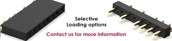
(B) Finish: Selective gold flash contact area/tin on tail - Under Plate: Nickel 50-100µ”
(C) Finish: Tin All Over – 80µ” minimum – Under Plate: Nickel 30-50µ”
(G&I) Finish: Gold 10µ” (G) or 30µ” (I) on contact area. Tin 100µ” minimum on tail - Under Plate: Nickel 50-100µ”Electrical
Current Rating: 1 AMP
Contact Resistance: 20mΩ Max.
Insulation resistance: 1000 MΩ MIN.
Dielectric withstanding voltage: AC 300 VEnvironmental and Processing
Operating Temperature: -40°C to +105°C - (Contact GCT if you require temperatures outside this range)
LCP Suitable For: IR Reflow, Wave, Manual solder
Be in the know about product launches, promotions and more
By submitting your email, you are agreeing to receive occasional updates from GCT.
Useful
Support
Global headquarters
GCT Limited
GCT Inc
GCT Hong Kong Ltd
Regional offices

Copyright © 2024 GCT (Global Connector Technology) All Rights Reserved